Topographic Sculpture of Kansas

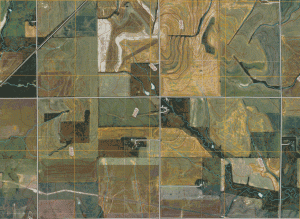
SchepmannFarmTopoMy friend Dan, who helped me build the light pipe prototype, recently got a CNC mill. He’s been asking me if there’s anything I want to make with it, and now I think I have an idea.

My in-laws live on a farm close to Holyrood, Kansas, damn near the geographic center of the United States. I thought it’d be cool to use the mill to carve, out of wood, a topographic representation of the land around the farm. Now, this being Kansas, there isn’t much change in elevation, but there are some pretty streams and enough variation, I think, to be interesting if we tweak the scale a bit.

Inspiration for this project came from jewelry designer, Erik Maes, who makes very cool topographic belt buckles.

Posted in design, projects | Tagged , , , , | 1 Comment

Recent Stories: Cyborgs, Solar, and Data Storage

This post is a roundup of the stories I’ve written over the past few weeks.

Without doing it consciously, I’ve totally carved out a cyborg beat. The most recent story is about a neural implant that is wirelessly controlled and wirelessly powered. The researchers, led by Brian Otis at the University of Washington, hope to implant this in humans someday, but have so far just demonstrated the sensor on a moth.

Another cool human-computer interface story I did was about a Microsoft Research project that uses muscle electrodes to interact with a computer. The main researcher, Desney Tan, is really trying to make muscle sensors cheap and easy to use so that the group’s prototype can eventually turn into something commercial. An awesome video of the technology, where a person plays Guitar Hero without the guitar, is here .

For The Economist, I wrote an update on a project by Babak Parviz at the University of Washington. Parviz is building a bionic eye by adding electro-optic devices to a contact lens.

Side note: all of the above researchers know each other and are either currently collaborating or have worked together on projects in the past.

I’ve also written one story about solar energy, a more efficient photovoltaic that uses nanopatterns to trap light better. The really interesting thing about this research is the physics behind it. These nanopatterns convert three-dimensional waves of light into two-dimensional waves that are confined to the surface of a metal. This process makes sunlight easier to turn into usable energy. The key to this 3D to 2D conversion is a quasiparticle called a surface plasmon. I have a little crush on plasmons (ever since grad school!), so I’ll be writing more about these in the future. Stay tuned!

Another piece I wrote was about researchers at Rice who use graphite–the same stuff that’s in pencils–to make a new type of chip-based memory that can hold more data than flash.

I covered research from NIST in which scientists developed a technique to scale up quantum computers, hopefully making them more practical.

And finally, I wrote about Intel’s announcement of an optical cable that the company would like to eventually replace the slow and heavy copper wires that people use to connect their computers, televisions, peripherals, etc. together. (For some background and more info on this topic, check out a post I wrote a while back.)

Posted in science, technology, writing | Tagged , , , , , , , , , , , , , , , , , | Comments Off on Recent Stories: Cyborgs, Solar, and Data Storage

Superconductor Levitation

This one’s from the e-vaults. I spent my first year of grad school making up undergraduate physics classes because I came in with a chemistry degree. One of those requirements was a laboratory class where we did things like measure the resistance of materials as a function of temperature. It wasn’t as dull as most of the labs because we got to play around with a Yttrium-Barium-Copper (YBC) superconductor. At liquid nitrogen temperatures-−321 °F–YBC was able to levitate a magnet. Fun! Below are two little videos of superconductor levitation:

The magnet spins above the superconductor, wrapped in masking tape and sitting in a well of liquid nitrogen. The wires are for measuring resistance and reading the temperature of the superconductor.

Posted in physics, science | Tagged , , , , , , | Comments Off on Superconductor Levitation

Exaflops on Beams of Light

A colleague of mine, Katie Bourzac, has written a post about the future of supercomputing according to IBM. Yes, the future is light. Essentially, the only way to find enough bandwidth to transport all the data required for future supercomputers is to use photons in waveguides, not electrons in wires.

The problem, however, is that it’s far too expensive to stick today’s lasers, detectors, modulators, amplifiers, etc. into computers. These devices are used to send data through the optical fiber that connects the world to the Web, but they are made of materials that are relatively expensive like indium gallium arsenide and others. There’s good news, though, for those who love supercomputers (and really, even if you don’t know you do, you totally do): there are a number of companies, including IBM and Intel, that are looking at using silicon–the same material found in electronics everywhere– for photonic devices.

If you know anything about bandgaps and optical properties of materials, you know that using silicon for photonics sounds a little crazy, but within the past five years, researchers have come up with engineering work-arounds that have made silicon feasible . And because silicon is at the heart of the electronics industry, and there’s a whole manufacturing infrastructure built around it, huge quantities of electronics can be churned out relatively quickly. Soon, photonic devices made of silicon could be churned out just as fast, and at such volume that their prices plummet. That’s when they can be integrated into computers and eventually chips.

It’ll take some time–some say at least a decade–but the gears have already been set in motion. Intel, for example, is pushing its photonics research into the market.  The company recently announced Light Peak, an optical cable that attaches a personal computer to peripherals, shuttling data at 10 gigabits per second. The first versions will contain old-school optics made with expensive materials. But Mario Paniccia, head of Intel’s Photonics Technology Lab hopes that Light Peak will be the Trojan horse to get photonics into the electronics industry; future versions will likely use silicon photonic parts.

Silicon photonics is a topic I’ve covered extensively for Technology Review. For the curious, here’s a link. I’ll continue to follow the work in the field because, from what I’ve seen, it’s the only way to keep pushing computation speeds. Also, it’s just so nerdy cool.

Posted in lasers, physics, science, technology | Tagged , , , , , , | 2 Comments